The bus
The key design parameter here was expediency. From the processor, through the buffers, to the DIN 41612 connector. Yes, I buffered everything. Overkill, maybe, but in that era you only shorted a pin to ground once to blow the output driver, chips these days are much more forgiving. And cheaper. I used bidirectional (74LS245) drivers throughout. The pinout of the 74LS244 unidirectional driver is a pain, routing was a lot easier with '245s hard-wired to go in one direction only (Actually, single-sided routing with '244s would have been impossible).
| C | A | |
|---|---|---|
| +5V | 1 | +5V |
| D0 | 2 | D1 |
| D2 | 3 | D3 |
| D4 | 4 | D5 |
| D6 | 5 | D7 |
| D8 | 6 | D9 |
| D10 | 7 | D11 |
| D12 | 8 | D13 |
| D14 | 9 | D15 |
| A23 | 10 | A22 |
| A21 | 11 | A20 |
| A19 | 12 | A18 |
| A17 | 13 | A16 |
| A15 | 14 | A14 |
| A13 | 15 | A12 |
| A11 | 16 | A10 |
| A9 | 17 | A8 |
| A7 | 18 | A6 |
| A5 | 19 | A4 |
| A3 | 20 | A2 |
| A1 | 21 | R/W |
| /LDS | 22 | /UDS |
| /AS | 23 | /VMA |
| /IACK | 24 | /IOSEL |
| /DTACK | 25 | /BR |
| /BG | 26 | /BGACK |
| E | 27 | /VPA |
| CK | 28 | /RESET |
| /6800INT | 29 | /IRQ1 |
| /IRQ2/3 | 30 | /IRQ4 |
| /IRQ5 | 31 | /IRQ6 |
| 0V | 32 | 0V |
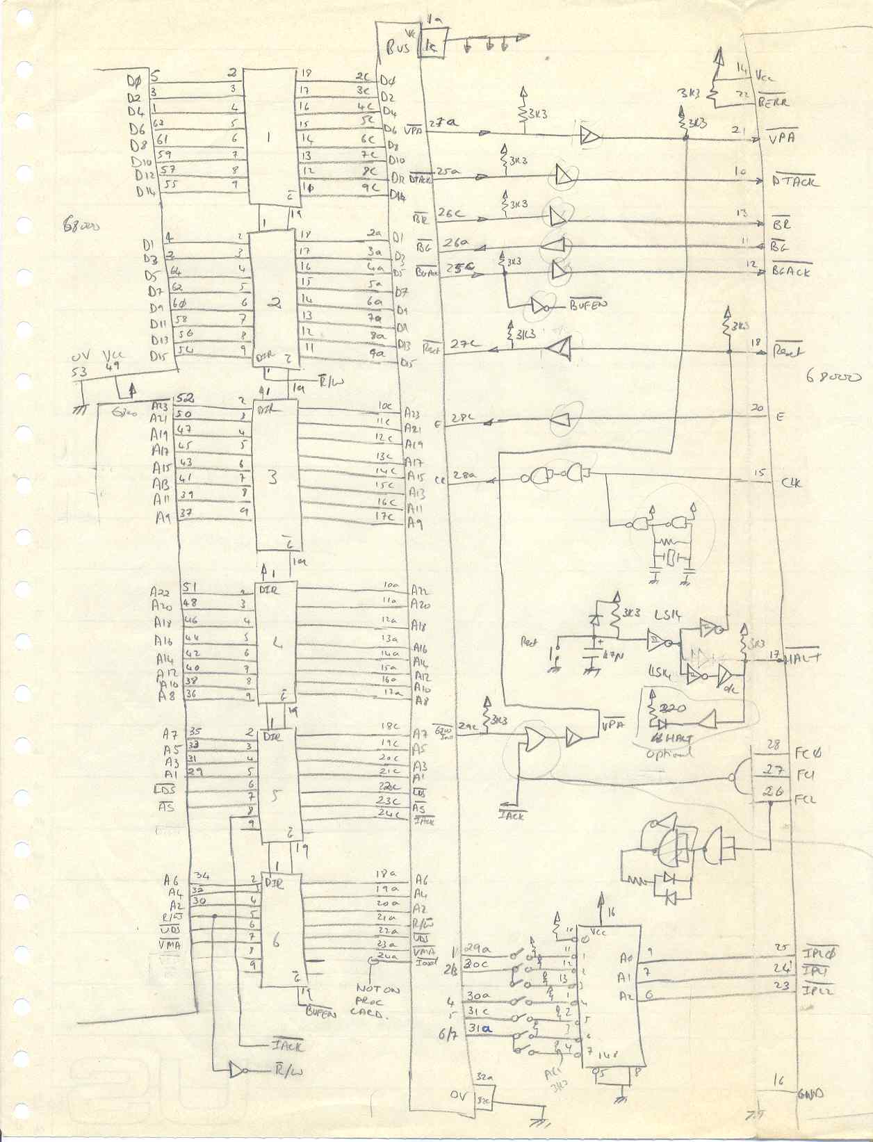
CPU board
68000, Interrupt logic, clock, buffers on all data and address lines.
Hand-drawn schematic, of course. I don't think there ever was a final version, but this is close. Changes would mostly have involved mapping gates into packages so that everything fitted on the PCB and could be routed.

This is the CPU PCB plot, with component overlay. Everything had to be checked by hand, smARTWORK didn't do netlists.
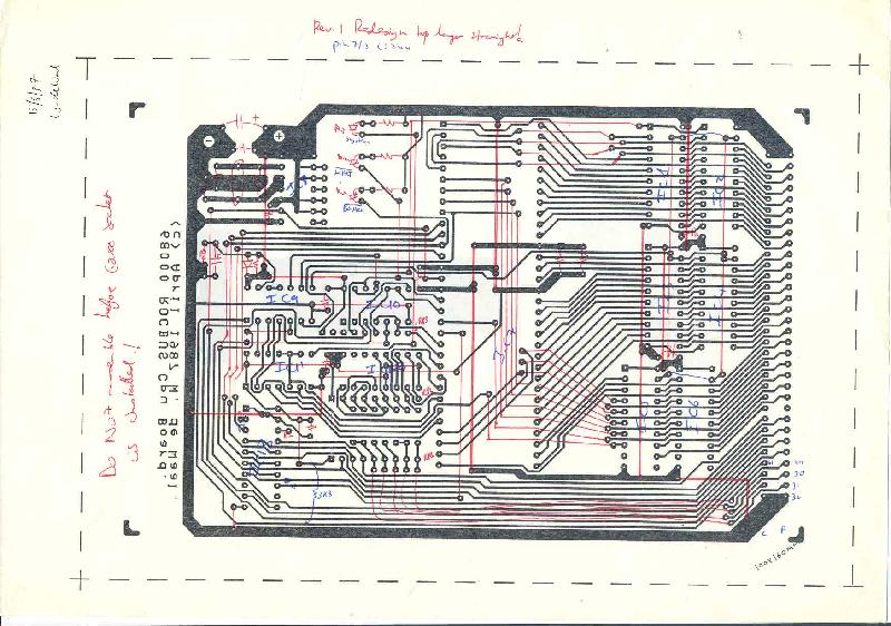

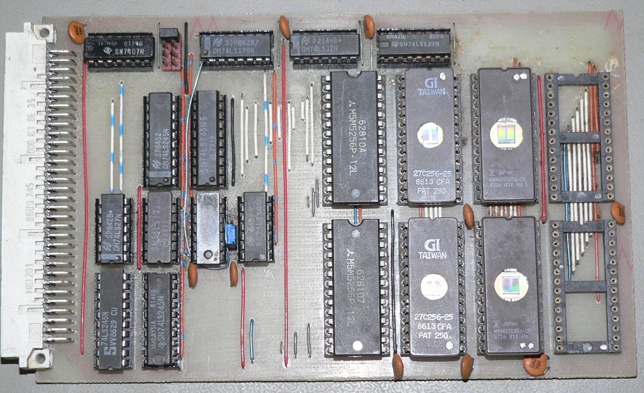
CPU Board, April 1987
Memory
Another Eurocard, with eight 256 kilobit devices -- two 42256 32k x 8 CMOS RAM chips and two, four or six 27C256 32k x 8 EPROMs, for 64K of RAM and 192K of ROM. Yes, only a few of the pictures* on this page will fit into that much (little?) RAM. Moore's law at work.
* And I mean one at a time.
Anyway. The 68000 was different from the Motorola 8-bitters that preceded it. In the case of the 6800, 6809, 6502 and so on, the reset vector lives at the top of memory, at FFFE/FFFF. These two bytes are read into the Program Counter on reset, and program execution then begins at that address.
The 68000, however, stores the initial Stack Pointer and Program Counter at 0x00000000 (16 bit address) to 0x00000007 (eight bytes, two 32-bit addresses). This is followed by pointers to all the exception handlers, including the Interrupt Pointers. It is nice*, but not essential, to use writeable memory so that the exception address can be changed (another option would be to point each exception at a bit of code in Read-Only Memory (ROM) which then fetches a vector from somewhere else. Cumbersome).
* Also, the 68000 has a short form for accessing memory in the first 32k (words) of address space, so it's a bit faster if you use this short form access for commonly used variables.
So, we need a bit of circuitry to make sure there's ROM at 0x00000000 for the first four cycles, and then to change things around so that the whole area maps to RAM (another approach would be to completely decode the address space and to map ROM to 0x00000000 to 0x00000007 and RAM from there on up, but the cycle counting approach is simpler). This is done with a 74LS164 shift register. The input is tied high (= "1") and the register is cleared at reset. With each address strobe, the 1 advances, eventually gets to the address decoder and changes the mapping (This comes straight from Motorola Application Note AN-897 except that the fourth output is used and not the eight, since the 68008 takes twice as long to fetch memory eight bits at a time).
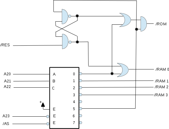
A note on the side: From the Hackaday 68000 Backplane Computer discussion I learnt that there's another (arguably better) approach (schematic) to the problem -- map a flip-flop to RESET and to the ROM chip select. The first time ROM is selected, the mapping flips and 0x00000000 is mapped to RAM.
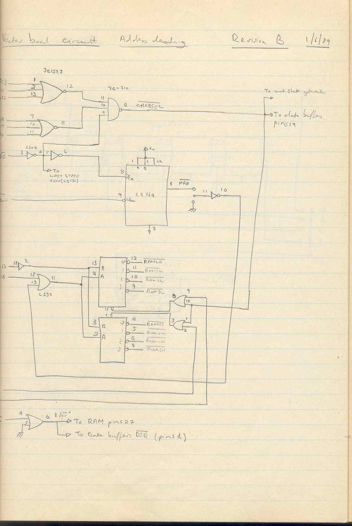
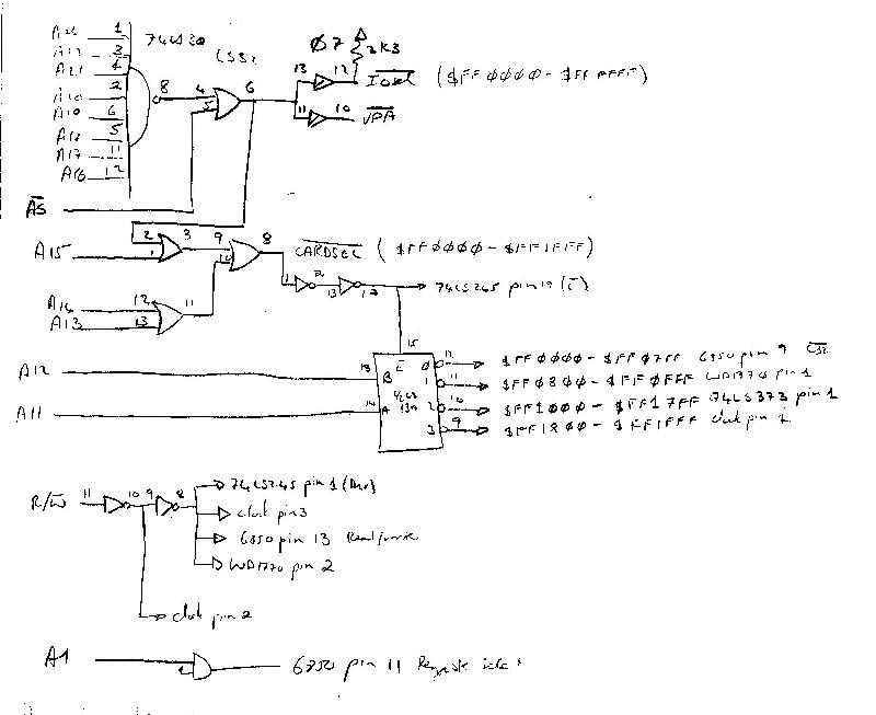
Schematic, part 1. From the top left hand side: A23, A21, A22, A18, A19, A20 (the order is of course to make routing easier) and /AS are used to generate /CARDSEL (0x0000000 to 0x0003FFFF, 256 kilobytes. Although the 68k architecture allows for a full 32 bit address bus, the 68000 only uses 24 address bits, something which caused great chaos when the Apple Macintosh got a processor capable of addressing more than 16 megabytes). Effectively, address lines 24-31 are ignored.
/AS and /RESET tickle the LS164 counter, as previously mentioned.
A17 is buffered, since it goes to two inputs on the LS139 address decoder. It works out well, because in the end there are exactly 16 address lines that needs to be buffered (Here's the schematic of the buffers for what it's worth -- the only slightly odd thing is that 68000 A1 goes to ROM/RAM A0, because of course 68000 A0 drives /LDS and /UDS which select one of the two devices). A16 is OR-ed with the MAP signal, giving:
| A17 | A16 | /MAP | MAP | LS37 pin 11 | Device selected |
|---|---|---|---|---|---|
| 0 | 0 | 0 | 1 | 1 | 1 - ROM 1 |
| 0 | 1 | 0 | 1 | 1 | 1 - ROM 1 |
| 1 | 0 | 0 | 1 | 1 | 3 - ROM 3 |
| 1 | 1 | 0 | 1 | 1 | 3 - ROM 3 |
| 0 | 0 | 1 | 0 | 0 | 0 - RAM |
| 0 | 1 | 1 | 0 | 1 | 1 - ROM 1 |
| 1 | 0 | 1 | 0 | 0 | 2 - ROM 2 |
| 1 | 1 | 1 | 0 | 1 | 3 - ROM 3 |
For the first four cycles after reset, A16 and A17 will be zero, so only the first entry and the last four entries are relevant. The other three Can't Happen.
What else? /UDS and /LDS are OR-ed with /CARDSEL to select between the LO and HI banks (because the 27C256 EPROM and 42256 RAM devices are eight bit, you need two per bank). And R/W is buffered with an OR gate because (1) there are no more free buffers after the 16 address lines mentioned above are buffered and (2) there's a spare OR gate. Elegant, if I say so myself.
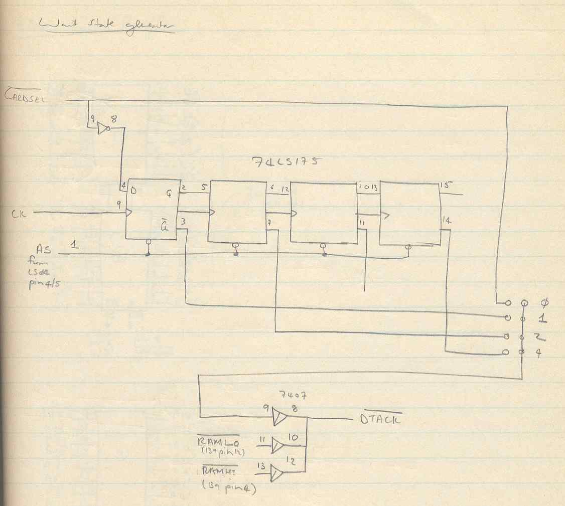
And then there's the wait state generator. The CMOS RAM is fast enough to keep up with the 68000, but the EPROM isn't. The wait state generator is four flip-flops being held in reset by /AS, inverted. When /AS goes low, the flip-flops start clocking the state of /CARDSEL through, i.e. nothing happens unless the decoding circuitry decides that 0x00000000 to 0x003FFFFF is being accessed). The jumpers on the right hand side determine when /DTACK is asserted to let the processor know it's OK to read data. Since /DTACK is driven from many sources, a 7407 open collector buffer is used here. And since we don't need wait states for RAM, selecting either RAM chip drives /DTACK via one of the other open collector gates.
If I were to do the same thing today, I would strongly consider using a PAL (the technology was available at the time, I just didn't want to complicate matters). Using a PAL would allow the RAM to be mapped at 0x000xxxxx and the EPROMs to all be mapped at 0x00Fxxxxx leaving the whole address space free for RAM expansion. But in those days 640k was still enough for everybody (not really, but it was and still is enough for this tinkerer).
Memory Board, June 1987 | No I didn't cover the EPROM windows to erase-protect them. But believe it or not, the data is still good, 20+ years later. |
I/O
Of course one needs I/O as well. I figured that a serial port would have to do for starters, graphics could come later.
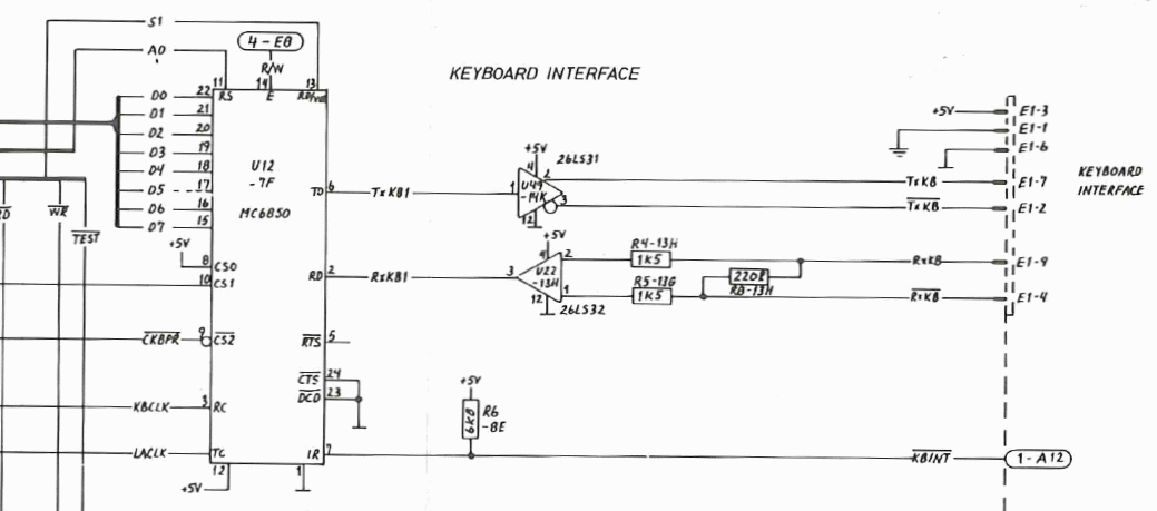
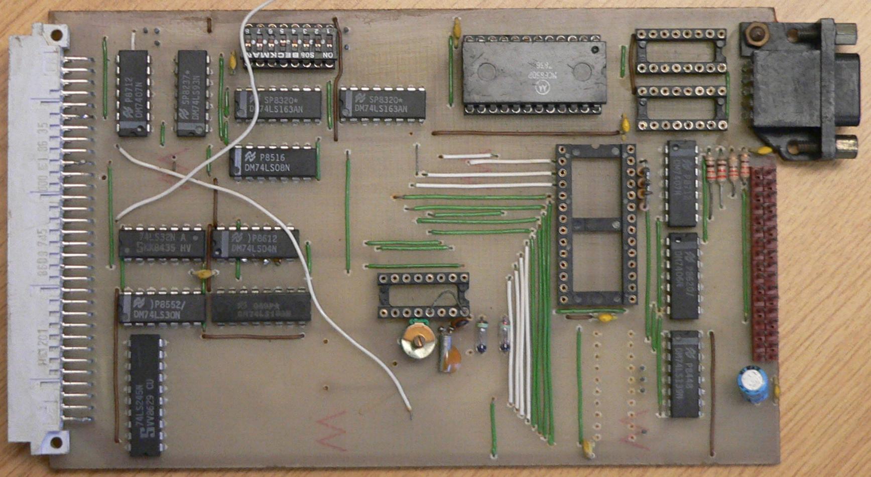
My first I/O board has a 6850 UART, a WD1770 floppy controller, and a 58174 real-time clock.
I don't know why I put two inverters there between the OR gate and the LS139 enable. As soon as I get around to it I will take them out of the circuit and wire one of them in on A16 to remap the board to FExxxx so that I can use it and the second board (see further down) at the same time.
Each I/O device takes up two kilobytes of memory -- far more than is needed, but it saved a whole lot of TTL. This issue was fixed in the next iteration.
At the time I figured that RS422 was the way to go, so that's what I used (remember that the Macintosh was new, and it used RS-422. Also, I didn't want to have to supply +12V and -12V just for the serial port (or rather, I didn't want to lose two pins on the backplane, a much bigger issue)).
I fitted one of these, but then kind of remembered I had a Tandberg TDV 2200 keyboard stashed away and that speaks RS-422, so I need to split the Tx (2400 bps) and Rx (600 bps) clocks and I can use the 6850 for my keyboard interface, just like the Tandberg does.
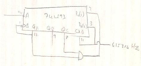
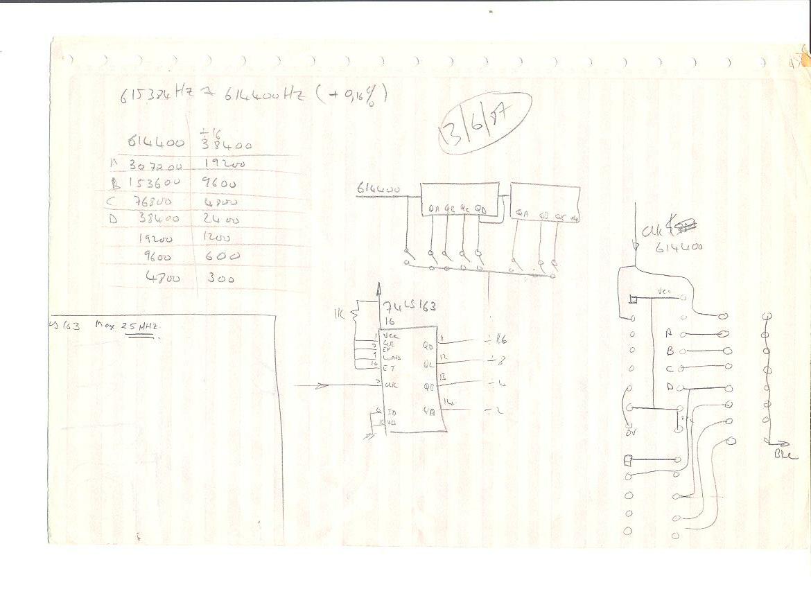
The Baud Rate Generator uses a 74LS93 and one AND gate to form a divide by 13 counter, which feeds two cascaded 74LS163 counters. The 615 kHz output can be used (in x16 mode) to generate 38.4 kbps, the first seven outputs of the dividers then give everything down to 300 baud.
First I/O Board, June 1987
Second I/O Board
In January 1989 I did some holiday work work (a requirement, then, when studying engineering) at Truvelo. There they had a Motorola MVME101 system they used for software development, and I ripped a copy of the ROM and the manual for it. I later found that this monitor is very similar to TUTOR and TUTORNEW for the Motorola M68000 Educational Computer Board -- but of course back then I didn't have access to the TUTOR sources.
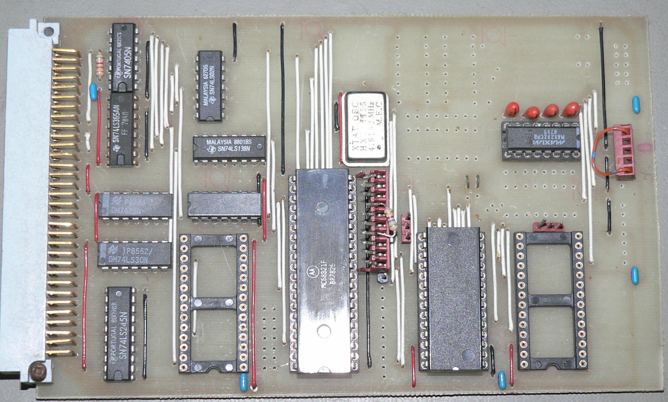
Now having a copy of MVME101BUG, my I/O requirements became 6840 PTM, 6821 PIA and 2 x MC68661 EPCI (UART) devices (I used an SCN2661B but it's the same thing). So I designed a second I/O board.
Update 2023-03-20: Obtained a pukka MC68661PC from Mantech. Works fine, except the A, B and C versions of this chip have different baud rate generator dividers. Fortunately one of the options is 0b1111 for divide- by-16, which will give me 19200 bps with the 4.9152 MHz clock.
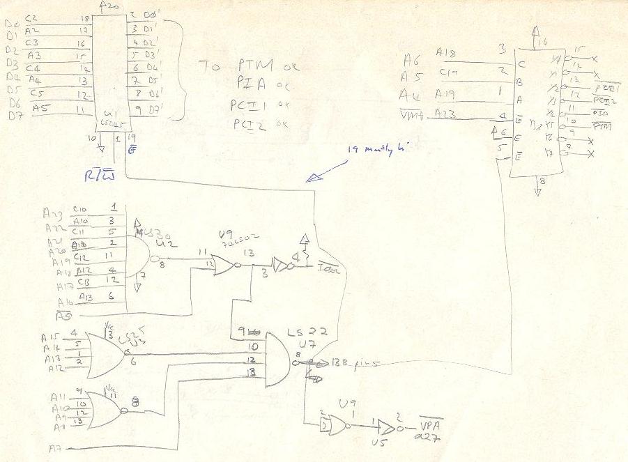
There's nothing interesting here really, the devices are mapped to 0x00FF0080 to 0x00FF00FF (The MVME101 maps these to 0x00FE00xx but I had this thing about minimising the memory footprint of I/O devices. Also, it saves an inverter, all the high address lines go straight to a 74LS30. In hindsight this doesn't matter that much).
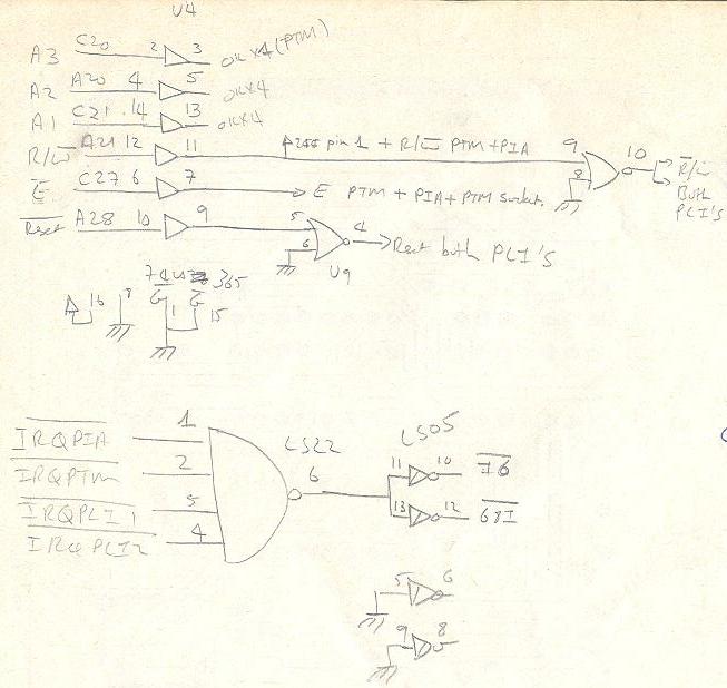
Spot the omission. Not that easy, since it's a partial schematic, but the inputs to the LS20 all need pull-up resistors, all the interrupt sources are open collector. Easily fixed these days with a handful of 0805s. And yes, I know I labelled it "LS22" that's probably before I added the LS05 buffer because of course the LS22 is open collector and we don't want that here.
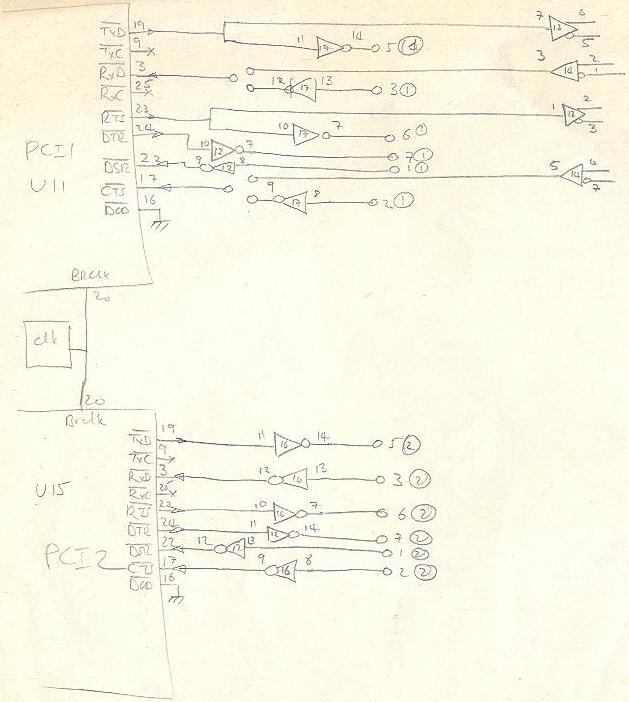
By now they'd invented the MAX232 (introduced 1987) and that's what I used to get RS-232. But I kept the RS-422 option. I used three MAX232s, one per port, the third being optional to give DTR and DSR for both serial ports.
That was then, these days I interface the raw TTL to a USB dongle, no line drivers required.
|
/DTR
/DTR |
Not shown, the 6840. Nothing to see, really, I brought the timer control pins out to a header and left that there, the timer can run on the E clock.
Software Development
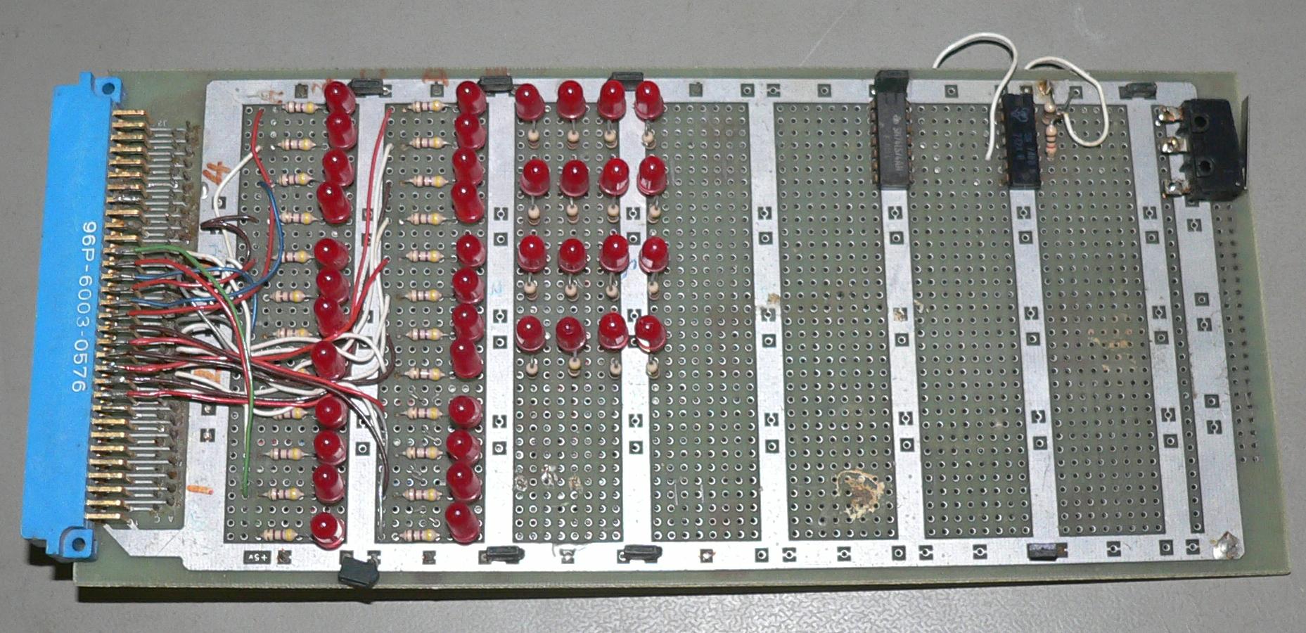
In the beginning the software development cycle was fun. (OK, so I'm a masochist :-). I used to write assembler code, hand-compile it, type it into a PC, burn two EPROMs, and then take the EPROMs home and stick them in the system. Single-stepping the 68000 is easy since the whole chip is CMOS. The 68K will wait for the data acknowledge signal DTACK forever. I built this fourth board on a wire-wrap card with LEDs on all data and address lines, and a flip-flop wired to a switch to take DTACK low for one cycle at a time. Removed the jumper on the memory card that selects the number of wait states when EPROM is selected, and I could single-step through EPROM while RAM accesses happened in the background. Yes, I could have used a bunch of hex to 7-segment decoders and displays but (1) the majority of 74xx and 40xx / 45xx decoders operate on BCD only, not hex, and (2) at this stage of my life I was as fluent in binary as in decimal, so it was no hardship reading the address and data (even now, 30+ years later, it's not that difficult).
I got a small monitor working this way, but I wouldn't recommend it :-). I wrote my own disassembler in C, and after I had got hold of a copy of Dr. Dobbs Toolbook of 68000 Programming I typed in the Tiny Basic interpreter which works well. I wanted to put Forth on there, but I got busy with other things, so it never happened.
So here we are in the 21st Century and I am again playing with this hardware. Single-stepping became a lot easier once I got MVME101bug working, and I now have a choice of assemblers (I use Quelo in DOSBox). Getting the code to the target is also easy, MVMEBUG has an undocumented feature where you can tell it to load S-Records from port 1 (This is documented for TUTOR and works the same in MVMEBUG).
MVME101bug 3.1 > LO1;X
(PASTE)
S00C0000433A3337332E484558C6
S120200021FC00000000090011FC000109034EB90000203A4EB90000202E11FC00BC
S120201D0009034EB90000203A4EB90000202E60DA203C0003640C538066FC4E75DF
S120203A48A7C0004E7110380902C03C0001EF40120010380901C03C0001ED408288
S12020570010380903C03C0001E540820010380900C03C0002820013C100FF2801A3
S10920744C9F00034E75B1
S9030000FC
MVME101bug 3.1 > md 2000 20;DI
002000    21FC000000000900     MOVE.L  #0,$00000900
002008    11FC00010903         MOVE.B  #1,$00000903
00200E    4EB90000203A         JSR     $0000203A
002014    4EB90000202E         JSR     $0000202E
00201A    11FC00542400         MOVE.B  #84,$00002400
[...]
- Get the 6850 working. AN-817 is seriously bad.
- Interrupt driven 6850 echo.
- Blinky light with delay loop.
TUTOR vs TUTORNEW
For the record, I took the time to compare the TUTOR source to TUTORNEW and other than being formatted for different assemblers, the differences are:
- COMMANDS: Version Number 2.1.1 instead of 1.3, obviously
- E: A routine FORCEUP to force characters entered to upper case, also called from MDDI, MMDI, OF, PF
- MS: A three-line bugfix of some type
- PF: Support for 68681 (TUTORNEW) at $EFFC01 instead of 6850 (TUTOR) at $010040
- TM: Updates to Transparent Mode, also 68661 related?
- TRAP14: Tape routine vectors removed
- W: Abort button support removed
- X: OUTCH streamlined
- Y: Tape support removed, streamlined, changes to initialisation
Dynamic RAM (insert icon of man digging trench here, remind everyone of the happy days of Geocities)
Interfacing the 68000 to dynamic RAM is actually quite easy -- see Figures 18 and 19 on PDF page 9 of Designing with Dynamic Memory from Electronics and Wireless World August 1986.
What caught me out is how ridiculously fast modern DRAM is. You see, I happened across a 16 MB 72 pin stick of RAM, with eight HY5117400 4 meg x 4 bit chips. One stick that provides as much memory as the 68000 can address? And it "hidden" refreshes itself? Works for me.
But see pages 4 and 11 of the datasheet -- tRCD(18) can be as little as 20ns but can not be more than 45 ns for this specific device. The E&WW example has a tRCD of 125 ns assuming an 8 MHz clock.
Fortunately, Dallas / Maxim makes a nifty 5-step digital delay line which will clock things along every 20ns and keep everyone happy (I hope).
More when I get around to it.
IDE
ISA Interface
Thanks for your interest,
In the following lines I describe how to interface an ISA
16bits wide peripheral to a M68K family member, I would like to
know if this sounds right, any comments, ideas or even examples
will be greatly appreciated..
I want to interface an ISA 16bit wide peripheral to an 68K
family microcontroller. In order to do this, I'm using two separate
address decoders (one for io-space and the other for the memory
space) and I connected the databus without any bridges together.
(I'm prepared to swap bytes to get the Endian right). I also generated
the following ISA bus signals:
ISA             68K
-------------------------------------------------------------
bale:           !as
iord:           !(!cs_io_space & r/w) (cs is active low)
iowr:           !(!cs_io_space & !r/w) (cs is active low)
mrd:           !(!cs_mem_space & r/w) (cs is active low)
mwr:           !(!cs_mem_space & !r/w) (cs is active low)
sbhe:           siz0 exor a0
And the other way around involves the following 68k signals:
68K             ISA
-------------------------------------------------------------
dsack1          chrdy terminates a waitstate generator which
                is started by cs_mem_space or cs_io_space,
                when the waitstate generator terminates, dsack1
                is asserted.
irq6            !int (tristated when not active low)
Thanks in advance,
Bart Nabbe
- PT68K (68000) (+ 68681, 68230, WD1772, WD1002, MK48T02)
- Blitz (68030) (+ 37C65, ATA)
- Ingo Cyliax / cs.indiana (68030) (+ 68901)
Overclocking
 | Using a 32 MHz clock module and a dual flip flop to get to 8 MHz meant I had two overclocking options, namely 16 MHz and 32 MHz. 16 MHz actually worked. 32 MHz... didn't. |
| 1476 hits since 1999-05-27. | Back to Wouter's 68000 Page | (This page last modified 2023-12-17) |